C256 Overview
Jump to navigation
Jump to search
| F256JR | C256-FMX | C256U | A2560U | A2560K | Gen-X | |
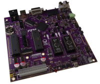
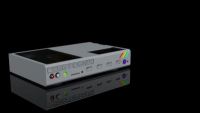
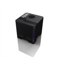
| F256 Jr. | C256 Foenix FMX (legacy) | C256 Foenix U/U+ | A2560 Foenix U/U+ | A2560K | GEN X | |
 |
 |
 |

|
 |

| |
| Released Year: | 2022/2023 | 2019 | 2021 | 2021/2022 | 2021 | 2022 |
| Active: | Yes | Discontinued | On Hold* | On Hold* | On Hold* | On Hold* |
| CPU: | W65C02 @ 6Mhz | W65C816 @ 14Mhz | W65C816 @ 14Mhz | MC68SEC000 @ 20Mhz | MC68040V @ 25Mhz | W65C816 @ 14Mhz + 32bits CPU** |
| System Memory: | 256K SRAM | 4M SRAM | 2/4M SRAM | 4M SRAM | 4M SRAM/64M SDRAM | 4M SRAM/64M SDRAM |
| Video Memory: | Shared | 4M SRAM | 2M SRAM | 2M SRAM | 8M SRAM | 8M SRAM |
| Graphic Chipset: | TinyVICKY - CFP9599 | VICKY II + GABE | FATVICKY - CFP95168B | FATVICKY - CFP95171-68k | VICKY III - CFP95179K | VICKY III - CFP95179X |
| Internal Audio: | 2x PSG (Sn76489) | TBD | 1x Gideon SID | 1x Gideon SID | 2x GideonSID / 1x OPM / 1x OPN2 / 2x PSG | 1x OPM / 1x OPN2 / 2x PSG |
| External Audio: | 2x SID^^ | 1x OPL3/1x OPM /1x OPN2/ 1x OPL3 | 1x OPL3 | 1x OPL3 | 2x SID^^/1x OPM /1x OPN2/1x PSG/1x OPL3 | 2x SID^^/1x OPM/1x OPN2/1x PSG/1x OPL3 |
| CODEC : | TBD | 1x 48KHz | 1x 48KHz | 1x 48KHz | 1x 48KHz/1x 44.1KHz | 1x 48KHz/1x 44.1KHz |
| Audio I/O: | HP Jack/Line-Out | HP Jack/Line-In/Out | HP Jack/Line-Out | HP Jack/Line-Out | HP Jack/Line-In/Out | HP Jack/Line-In/Out |
| Media IO: | IEC/SDCARD | SDCARD/IDE/FLOPPY | SDCARD/IDE | SDCARD/IDE | SDCARD/IDE/FLOPPY | SDCARD/IDE/FLOPPY |
| COM IO: | Simple Serial/WIFI*** | 2x Serial/ 1x Parallel | 1x Simple Serial | 1x Simple Serial | 2x Serial/1x Parallel/Eth | 2x Serial/1x Parallel/Eth |
| Joystick Posts: | 2x ATARI + NES/SNES Port****^ | 4x ATARI / 2x NES/SNES^ | 2x ATARI And/Or NES/SNES^ | 2x ATARI And/Or NES/SNES^ | 2x ATARI And/Or NES/SNES^ | 4x ATARI & 4x NES & 4x SNES |
| PCB Form Factor: | 6.7" x 6.7" Mini-ITX | 10" x 6.2" | 7.13" x 4.4" | 7.13" x 4.4" | 12" x 5.5" | 9" x 9" |
| Power Supply: | ATX PS Plug | +12V 2.5mm Barrel | +12V 2.5mm Barrel | +12V 2.5mm Barrel | 4pins +5V/+12V | ATX PS Plug |
| Tech Manual: | JR TM Preliminary | NONE | TBP Later | A2560U UM Preliminary | A2560K UM Preliminary | Coming Soon |
| User Manual: | F256 JR UM (WIP) | NONE |
(*): Due to FPGA's availability and abusive cost, those models are presently on hold.
(**): The concept behind the GenX is its ability to support different processors through a modular system.
(***): The WIFI communication is achieved through a ESP32/WIFI (Feather) Type board and it is optional.
(****): The RevA of the board doesn't have an extra 9Pins connector to interface with NES/SNES Adapter.
(^): An external NES/SNES interface box is needed, so this is extra.
(^^): The External SIDs are Sockets only, they must be populated by the owner.
OPM = YM2151, OPN2 = YM2612, PSG = SN76489