Difference between revisions of "F256K"
HaydenKale (talk | contribs) |
HaydenKale (talk | contribs) |
||
| Line 73: | Line 73: | ||
= Keyboard = | = Keyboard = | ||
The built-in keyboard does not operate by PS/2 controller, it's a matrix keyboard controlled by two WDC VIA (Versatile Interface Adapter) controllers and the CPU's NMI signal. For the complete description of VIA, see [https://www.westerndesigncenter.com/wdc/documentation/w65c22.pdf WDC's specification]. | The built-in keyboard does not operate by PS/2 controller, it's a matrix keyboard controlled by two WDC VIA (Versatile Interface Adapter) controllers and the CPU's NMI signal. For the complete description of VIA, see [https://www.westerndesigncenter.com/wdc/documentation/w65c22.pdf WDC's specification]. | ||
| + | |||
| + | There are two ways for programs to interact with the keyboard: | ||
| + | * '''Using the kernel''', where the exact mechanism depends on the kernel involved | ||
| + | * '''Directly with the device''', using memory mappings. | ||
| + | |||
| + | For more information on interacting directly with the keyboard device, see [[F256K Keyboard]]. | ||
* '''Restore''' key is controlled by NMI signal. | * '''Restore''' key is controlled by NMI signal. | ||
Revision as of 17:40, 25 June 2023
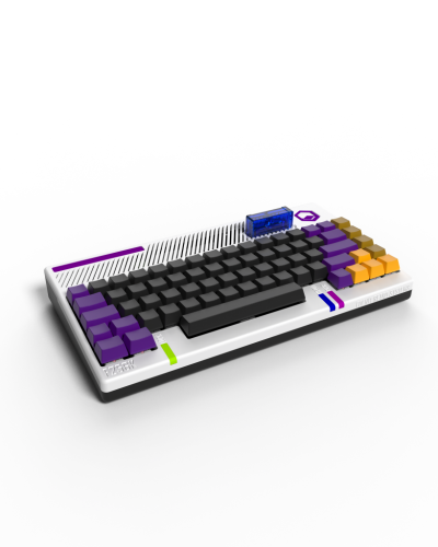
The F256K is a 65xx-based system. It's an encased form factor with a built-in keyboard. It includes the following features:
- 512K of Shared System & Video RAM
- 256k of flash
- 256k of cartridge ram/rom
- TinyVICKY Graphic Chip (CFP9599)
- Port for connecting FNX4N4S, which can be used to connect Atari-Style Joysticks or NES/SNES gamepads
- 1x IEC Port to interface to Commodore Drives
- SID sound chip
It shares many similarities to the F256JR and programs can in many cases run straightforwardly on both.
The 'K' in the name comes from the fact that it has an integrated keyboard, unrelated to the amount of memory available in the system. The base system has 512K of system memory; with expansion cartridge brings it up to 768K.
A common variety of the F256K uses the 6502 CPU. That said, the 65816 CPU can also be installed.
Ports and connectors
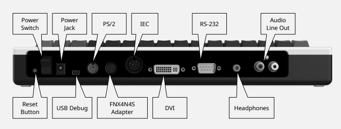
The back of the unit looks like this:
- Power Switch is a toggle-style switch to turn the unit off and on.
- Reset Button reboots the system, with values in RAM persisting. If RAM has been modified using the debug interface, it stays modified.
- Power Jack is for plugging in A/C power. Use, for example, a +12V or +9V with 2.5mm Barrel connector.
- USB Debug is for connection to a debug host computer, debugging F256K as a target, for example using a mini USB to USB A cable.
- PS/2 can be used for connecting external keyboard and/or mouse.
- FNX4N4S Adapter provides connections to gamepads (e.g., SNES-style game controller) through the FNX4N4S adapter.
- IEC provides connectivity to Commodore-compatible devices that use serial interface
- DVI is for connecting a display.
- RS-232 provides a standard RS-232 serial interface.
- Headphones is a standard 3.5mm headphone jack.
- Audio Line Out provides stereo audio output.
Switches
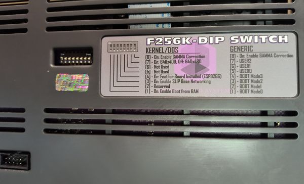
The bottom of the unit looks like this:
There are eight DIP switches, with different interpretations depending on whether a kernel is present on the system. If a kernel is present on the system, as the unit is shipped with, these switches are:
- [8] - On: Enable GAMMA correction
- [7] - Graphics resolution controls
- [6] - Not used
- [5] - Not used
- [4] - On: Feather Board installed (ESP8266)
- [3] - On: Enable SLIP Base Networking
- [2] - Reserved
- [1] - On: Enable Boot from RAM, off means it will boot from a pre-installed kernel in the first 48K of memory.
If a kernel is not present on the system, these switches can be used as desired:
- [8] - On: Enable GAMMA correction
- [7] - USER2
- [6] - USER1
- [5] - USER0
- [4] - BOOT Mode3
- [3] - BOOT Mode2
- [2] - BOOT Mode1
- [1] - BOOT Mode0
Boot
To start the machine, ensure A/C power is plugged in and flip the power switch. The exact boot behavior depends on the "Boot from RAM" DIP switch on the bottom.
If the DIP1 "Boot from RAM" switch is off and a kernel is used, the kernel will search the 48K of memory for a pre-loaded kernel binary.
If the DIP1 "Boot from RAM" switch is on, then control is transferred to the reset vector entrypoint located at offset $FFFC.
Switching DIP1 to 'on' is useful for developer convenience and testing code. For those using the machine outside of a development-style environment, it's more likely the switch will be 'off'.
Note: the "Boot from RAM" and "Boot from flash" options in uploader tools such as FoenixMgr or F256 Uploader are unrelated to the "Boot from RAM" DIP switch. The DIP swtich tells the kernel to search the first 48K of RAM for a pre-loaded kernel binary; those tools send a soft reset signal to reset to an entrypoint either in RAM or Flash memory respectively.
Keyboard
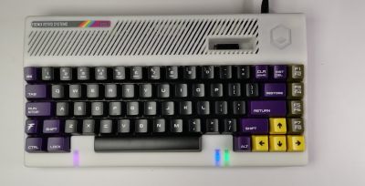
The built-in keyboard does not operate by PS/2 controller, it's a matrix keyboard controlled by two WDC VIA (Versatile Interface Adapter) controllers and the CPU's NMI signal. For the complete description of VIA, see WDC's specification.
There are two ways for programs to interact with the keyboard:
- Using the kernel, where the exact mechanism depends on the kernel involved
- Directly with the device, using memory mappings.
For more information on interacting directly with the keyboard device, see F256K Keyboard.
- Restore key is controlled by NMI signal.
- Right arrow and down arrow are controlled by VIA0.
- Rest of the keys are all controlled by VIA1.
The VIA controllers themselves are memory-mapped, visible to CPU I/O Page 0. They're memory-mapped to these locations:
VIA0_PRA  =  $dc01  ; VIA#0 (Port Register A)
VIA0_DDRA =  $dc03  ; VIA#0 (Data Direction Register A)

VIA0_PRB  =  $dc00  ; VIA#0 (Port Register B)
VIA0_DDRB =  $dc02  ; VIA#0 (Data Direction Register B)

VIA1_PRA  =  $db01  ; VIA#1 (Port Register A)
VIA1_DDRA =  $db03  ; VIA#1 (Data Direction Register A)

VIA1_PRB  =  $db00  ; VIA#1 (Port Register B)
VIA1_DDRB =  $db02  ; VIA#1 (Data Direction Register B)
The typical way to poll for the majority of the keys (i.e., all the keys except right arrow, down arrow, and Restore) is to write to VIA1 port A, then read from VIA1 port B. Functionally, you might observe the reverse to also work on hardware. That said, the role of port A is to short the pin while port B has pull-ups, therefore it is best for the health of the system components to write to port A and read from port B.
For example, to detect the user hitting the space bar, first initialize the keyboard as follows:
; Initialize matrix keyboard
; Designate port A for write, and port B for read.
LDA #$FF
STA VIA1_DDRA
LDA #$00
STA VIA1_DDRB
Then to poll for input, use
; Space is PB4, PA7
LDA #(1 << 7 ^ $FF)
STA VIA1_PRA
LDA VIA1_PRB
CMP #(1 << 4 ^ $FF)
BEQ SpaceBarPressed
For a more complete reference, see the manual.
Manual
For a technical reference, use this manual: https://github.com/pweingar/F256Manual
Although the manual is F256Jr-centric, it's suitable for F256K development owing to the similarity of the two units. It describes common aspects between F256Jr and F256K, with some sections highlighting F256K functionality that differs.
Kernels
There are three kernels for the F256K.
- The TinyCore MicroKernel (ships with the unit)
- OpenKERNAL (for those wishing to run software written for the CBM KERNAL)
- FoenixKERNAL, an open source, CBM-style layer also compatible with software written for Commodore 64 KERNAL


